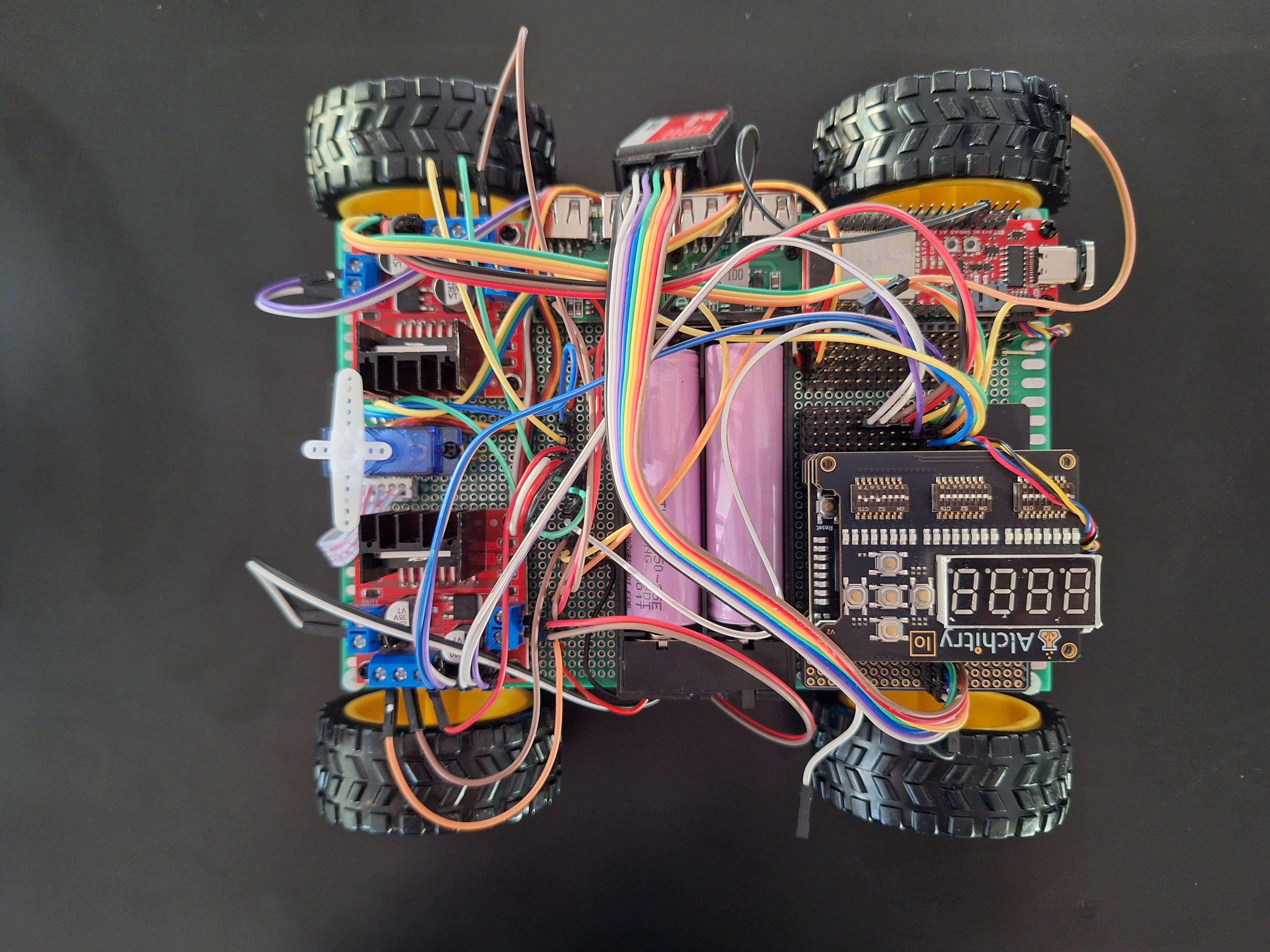
The FPGA robot consists of the following parts:
The specifications are found here.
The table below shows the GPIO pins that ESP32 board provides to the board edge and their Alchitry connections and uses:
| ESP32 | Alchitry | ||||
|---|---|---|---|---|---|
| GPIO # | Use | Pin # | Bank | Pin # | Use |
| 0 | Button | N/C | |||
| 1 | TX to CH340 RX | N/C | |||
| 2 | RGB LED | N/C | |||
| 3 | RX from CH340 TX | N/C | |||
| 4 | 28 | Camera Data 0 | |||
| 5 | uSD CS/ | N/C | |||
| 12 | 8 | Camera Data 1 | |||
| 13 | Blue LED | 9 | Camera Data 2 | ||
| 14 | 3 | Camera Data 3 | |||
| 15 | 5 | Camera Data 4 | |||
| 16 | RX | 26 | |||
| 17 | TX | 27 | |||
| 18 | SCK, uSD Card SCK | 23 | |||
| 19 | POCI, MISO, uSD Card MISO | 25 | |||
| 21 | SDA | 1 | I2C SDA | ||
| 22 | SCL | 2 | I2C SCL | ||
| 23 | PICO, MOSI, uSD Card CS/ | 24 | |||
| 25 | A1 | 18 | |||
| 26 | A0 | 17 | |||
| 27 | 7 | Camera Data 5 | |||
| 32 | 4 | Camera Data 6 | |||
| 33 | 6 | Camera Data 7 | |||
| 34 | A2 | 19 | |||
| 35 | A5 | 22 | V Sync | ||
| 36 | A4 | 21 | H Sync | ||
| 39 | A3 | 20 | Pixel Clock | ||
The System Verilog for the FPGA includes the following components:
The components above allow the FPGA robot to share line sensing, motor control and servo control firmware with the Freenove 4WD Car.
The FPGA is essentially the electronic equivalant of LEGO blocks. You use a programming language such as Verilog or System Verilog to describe how the blocks are connected together. An example AND gate in System Verilog is shown below:
|
Clocked logic such as flipflops use registers for features that get clocked. The different assignment symbol indicates the latched result after the device is clocked. The always statement describes the edge that latches the result. A flipflop example in System Verilog is shown below:
|
A tool such as Vivado is used to validate the System Verilog or Verilog input and convert it into a form that can be mapped onto the FPGA logic elements. The next step is to pick locations for the FPGA logic elements and route the signals between the FPGA logic elements and to and from the FPGA external pins. When the placement and routing is complete, the final step is to create a binary file that is used to tell the FPGA the desired configuration of the electronic LEGO blocks. After the binary file is loaded into the FPGA, the FPGA's behavior is specified by the Verilog code.
Debugging the FPGA code is done via simulator or looking at oscilliscope traces. The waveforms show how the input signals travel through the combinational and clocked logic to produce the desired outputs. Depending upon the number of available pins on the FPGA, it may be possible to route some internal signals to some debug output pins for debugging, allowing you to view the signals on an oscilliscope or logic analyzer.
Below are some of the resources for Verilog:
Here are some links that enable you to go further down the rabbit hole of building your own printed circuit board, Application Specific Integrated Circuit (ASIC) and Universal Serial Bus (USB).
Here are some printed circuit board design links:
Here are some MOSbius links:
Here are some ASIC design links:
Here are some USB links: